Research Stories
Development of a New Technology for 2D Transition Metal Chalcogenides
Successfully determined the synthetic techniques by overcoming the limitation using plasma
Mechanical Engineering
Prof.
KIM, TAESUNG
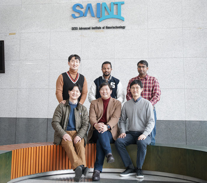
Prof. Ji Won Suk, Ph.D. Hyeong-U Kim

Prof. Kim, Taesung (School of mechanical engineering/SAINT) developed a new technology for two-dimensional (2D) transition metal chalcogenides (TMDs) for the first time in 2015 using plasma-enhanced chemical vapor deposition (PE-CVD) instead of SiOx and SiNx.
It is great significance in overcoming the limitations of conventional synthetic techniques (thermal chemical vapor deposition, mechanical exfoliation) such as high process temperature (>550 oC) and small dimensions (size a few cm). ICP type with shower type of nozzle can achieve high uniformity with 4-inch large size using PECVD. In addition, the high-density plasma of ICP has unique properties by inducing the nano size of grain.
From 2015 to the present, various 2D TMDs have been successfully synthesized using PE-CVD and many papers(※) and patents have been published. Also, this time, we succeeded in fabricating TMDs-TMDs heterostructure for 4-inch wafer scale. Prof. Taesung Kim’s group (Hyunho Seok, Chaitanya Kanade) and Dr. Hyeong-U Kim (KIMM) developed a new technology using the heterostructure of TMDs-TMDs with experience in synthesis know-how using PECVD. Moreover, Prof. Ji Won Seok’s group (Yonas T. Megra) analyzed the interfacial adhesion properties between the synthesized MoS2-WS2 heterostructures and substrates. It validates the structural stability of the interfaces between MoS2 and WS2.
Regarding this research, Prof. Kim said, “We can use cold plasma to overcome the limitations of conventional heterostructure fabrication such as, low uniformity and small size and can be applied to TMDs heterostructure research with high potential for mass production in the near future.”
A related research paper, ‘Low-Temperature Synthesis of Wafer-Scale MoS2-WS2 Vertical Heterostructures by Single-Step Penetrative Plasma Sulfurization’ was published in ‘ACS Nano’ (I.F.=14.588, JCR <10%). This research was supported by the National Research Foundation of Korea (NRF) 2018R1D1A1B07040292, 2017R1A2B3011222, and 2019R1A2C2089785.
※ PECVD 2D Materials Synthesis Related Papers (Prof. Kim, Taesung’s Group)
1) Low-Temperature Synthesis of Large-Scale Molybdenum Disulfide Thin Films Directly on a Plastic Substrate Using Plasma-Enhanced Chemical Vapor Deposition (H.-U. Kim et al., Advanced Materials, 27, 2015, 5223-5229)
2) Highly uniform wafer-scale synthesis of α-MoO3 by plasma enhanced chemical vapor deposition (H.-U. Kim et al., Nanotechnology, 28, 2017, 175601)
3) Low-temperature wafer-scale growth of MoS2-graphene heterostructures (H.-U. Kim et al., Applied Surface Science, 470, 2019, 129-134)
4) Wafer-Scale and Low-Temperature Growth of 1T-WS2 Film for Efficient and Stable Hydrogen Evolution Reaction (H.-U. Kim et al., Small, 16, 2020, 1905000)
5) Flexible MoS2–Polyimide Electrode for Electrochemical Biosensors and Their Applications for the Highly Sensitive Quantification of Endocrine Hormones: PTH, T3, and T4 (H.-U. Kim et al., Analytical Chemistry, 92, 2020, 6327-6333)
6) Realization of Wafer‐Scale 1T‐MoS2 Film for Efficient Hydrogen Evolution Reaction (H.-U. Kim et al., ChemSusChem, 2021) doi.org/10.1002/cssc.202002578
7) Low-Temperature and Large-Scale Production of Transition Metal Sulfide Vertical Heterostructure and Its Application for Photodetectors (Chaitanya et al., ACS Applied Materials & Interface, 2021)
8) Low-Temperature Synthesis of Wafer-Scale MoS2-WS2 Vertical Heterostructures by Single-Step Penetrative Plasma Sulfurization (H. Seok et al., ACS Nano, 15, 2021, 707-718)